


| Products>Semiconductor |

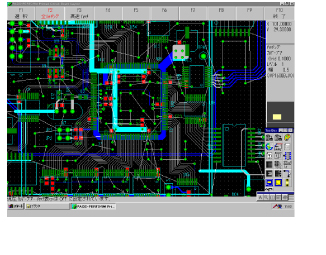 |
A substrate pattern will be designed quickly and for a low cost. | |||
| 1. | CAD used: PowerPCB | |||
| 2. | Required documents: Circuit plan, bill of materials, planned outside form of substrate, design requirements, product information, net list | |||
| 3. | Maximum substrate size: 1,397mm x 1,397mm | |||
| 4. | Maximum number of layers: 30 (with boards of 1.6mm thickness, maximum of 8) | |||
| 5. | Able to build with multiple layers on a single side. Also able to produce dual sided substrate chips. | |||

![]() Copyright © OOKUMA ELECTRONIC Co., Ltd. All rights reserved.
Copyright © OOKUMA ELECTRONIC Co., Ltd. All rights reserved.